The feature size and functional range of molecular electronic devices: Monitoring the transition from tunneling leakage current to molecular tunneling
Advances of miniaturization in electronics have created dramatic impacts on the industrial innovations and our lives. Nowadays, the semiconductor industry has been devoted to scaling down the feature size of electronic devices to the scale of sub-5 nm. Moore's Law, however, has not been the only priority in semiconductor industry because of some inevitable quantum obstacles which hinder the further miniaturization and integration, such as the tunneling leakage current and the thermal dissipation. As a candidate of the supplementary support and even replacement for future electronic device, the bottom-up strategy to use single molecules as charge transport component can be promising, as the primary molecular elements for building single-molecule electronic components in electronic circuitry possess the intrinsic charge transport properties to overcome the tunneling leakage between the same scale of nanogap distance. Nevertheless, knowing the feature size of the domination of tunneling leakage in molecular electronics is of fundamental significance, which enhances the understanding of the technical limitations and boundaries for using single-molecule components as electronic devices.
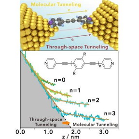
By employing a series of oligo(aryleneethynylene) (OAE) derivatives with different numbers of repeating units of ethynylphenyl as molecular ruler, we used mechanically controllable break junction technique to investigate the dominant size ranges of the through-space tunneling (tunneling leakage between the source and drain electrode) and molecular tunneling of single-molecule junctions. To avoid the inevitable snap-back effect during the electrode stretching, which might hinder the detection of some molecular junction configurations at the initial stage of gap opening, we chose the electrode gap closing process to provide precise determination of the electrode-electrode distance for the conductance-nanogap size correlation. Hence, by screening this series of OAE molecules, a correlation of the characterized conductance of the molecules with different lengths and configurations is investigated, and the transition between through-space tunneling and molecular tunneling is quantitatively determined.

The tunneling leakage is a major quantum obstacle which hinders further miniaturization of electronic devices. To explore the miniaturization limits of molecular electronics, the oligo(aryleneethynylene) (OAE) molecules were employed to investigate the transition between through-space tunneling and molecular tunneling. For the shortest OAE molecule, the intrinsic single-molecule charge transport can be outstripped from tunneling leakage at 0.66 nm, suggesting the potential to push the miniaturization limit of molecular electronic devices to the angstrom scale.
By retrieving the most probable conductance-distance evolution from conductance-distance histogram of molecular junction, which we called "master curve", we found direct transition between through-space dominated transport and molecular tunneling dominated transport. Therefore, with the molecular length increases, the effective nanogap distance range where the single-molecule devices properly function, which the molecular tunneling dominated, for each OAE molecule is 0.66~1.2 nm for OAE2, 0.91~1.9 nm for OAE3, 1.2~2.5 nm for OAE4 and 1.5~3.3 nm for OAE5, respectively. These findings suggest that in future single-molecule electronics, to use the intrinsic properties of the target molecules, nanogaps within two terminals must reach a certain range of size according to the target molecules to outstrip the tunneling leakage current. On the other hand, for the smallest OAE2, we obtained a feature size of below 0.66 nm, suggesting the shrinking limit for using molecular electronic device. "These conclusions suggest that assembling conjugated molecules with bottom up strategy for molecular electronics are highly promising for future miniaturization of electronic devices." says Junyang Liu, the first author of the study, who dose his postdoctoral research in Collaborative Innovation Center of Chemistry for Energy Materials, China.
Resource: Nanotechnology Now
- 333 reads
Human Rights
Fostering a More Humane World: The 28th Eurasian Economic Summi

Conscience, Hope, and Action: Keys to Global Peace and Sustainability

Ringing FOWPAL’s Peace Bell for the World:Nobel Peace Prize Laureates’ Visions and Actions

Protecting the World’s Cultural Diversity for a Sustainable Future

Puppet Show I International Friendship Day 2020

