Irregular silicon wafer breakage studied in real-time by direct and diffraction X-ray imaging
Fracture and breakage of single crystals, particularly of silicon wafers, are multi-scale problems: the crack tip starts propagating on an atomic scale with the breaking of chemical bonds, forms crack fronts through the crystal on the micrometre scale and ends macroscopically in catastrophic wafer shattering.

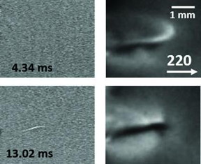
On the left are the direct transmission images. On the right are the diffraction images.
Total wafer breakage is a severe problem for the semiconductor industry not only during handling but also during temperature treatments, leading to million-dollar costs per annum in a device production line. Knowledge of the relevant dynamics governing perfect cleavage along the {111} or {110} faces, and of the deflection into higher indexed {hkl} faces of higher energy, is scarce due to the high velocity of the process. Imaging techniques are commonly limited to depicting only the state of a wafer before the crack and in the final state.
A group of researchers demonstrates, for the first time, in situ high-speed crack propagation under thermal stress, imaged simultaneously in direct transmission and diffraction X-ray imaging [Rack, Scheel and Danilewsky (2016). IUCrJ, 3, 108-114; doi:10.1107/S205225251502271X]. The scientists show how the propagating crack tip and the related strain field can be tracked in the phase-contrast and diffracted images, respectively. Movies with a time resolution of microseconds per frame reveal that the strain and crack tip do not propagate continuously or at a constant speed. Jumps in the crack tip position indicate pinning of the crack tip for about 1-2 ms followed by jumps faster than 2-6 m s-1, leading to a macroscopically observed average velocity of 0.028-0.055 m s-1. The results also give a proof of concept that the described X-ray technique is compatible with studying ultra-fast cracks up to the speed of sound.
Source: Nanotechnology Now
- 346 reads
Human Rights
Fostering a More Humane World: The 28th Eurasian Economic Summi

Conscience, Hope, and Action: Keys to Global Peace and Sustainability

Ringing FOWPAL’s Peace Bell for the World:Nobel Peace Prize Laureates’ Visions and Actions

Protecting the World’s Cultural Diversity for a Sustainable Future

Puppet Show I International Friendship Day 2020

