'Nano machine shop' shapes nanowires, ultrathin films
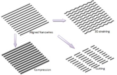
One-dimensional nanomaterials have attracted a great deal of research interest in the past few decades due to their unique mechanical, electrical and optical properties. Changing the shape of nanowires (NWs) is both challenging and crucial to change the property and open wide functions of NWs, such as strain engineering, electronic transport, mechanical properties, band structure and quantum properties, etc. Here we report a scalable strategy to conduct cutting, bending and periodic straining of NWs by making use of laser shock pressure. Three-dimensional shaping of silver NWs is demonstrated, during which the Ag NWs exhibit very good ductility (strain-to-failure reaches 110%). Meanwhile, the high electrical conductivity of Ag NWs could retain well under controlled laser shock pressure. The microstructure observation indicates that the main deformation mechanism in Ag NWs under dynamic loading is formation of twinning and stacking fault, while dislocation motion and pile-up is less obvious. This method could be applied to semiconductor NWs as well.
A new "nano machine shop" that shapes nanowires and ultrathin films could represent a future manufacturing method for tiny structures with potentially revolutionary properties.
This illustration depicts a new nano machine shop's ability to shape tiny wires, an advance that represents a possible future manufacturing method for applications ranging from high-speed electronics to solar cells.
The structures might be tuned for applications ranging from high-speed electronics to solar cells and also may have greater strength and unusual traits such as ultrahigh magnetism and "plasmonic resonance," which could lead to improved optics, computers and electronics.
The researchers used their technique to stamp nano- and microgears; form tiny circular shapes out of a material called graphene, an ultrathin sheet of carbon that holds promise for advanced technologies; and change the shape of silver nanowires, said Gary Cheng, an associate professor of industrial engineering at Purdue University.
"We do this shaping at room temperature and atmospheric pressure, like a nano-machine shop," said Cheng, who is working with doctoral students Ji Li, Yiliang Liao, Ting-Fung Chung and Sergey Suslov and physics professor Yong P. Chen.
Graphene and nanowires - filaments 1,000 times thinner than a human hair - have numerous potential applications. However, technologies are needed to tailor them for specific uses. The new method, called laser shock-induced shaping, makes it possible to tune nanowires by altering electrical and optoelectrical properties that are critical for electronic components.
The researchers also have shown how laser shock-induced shaping can be used to change the properties of graphene, a step toward harnessing the material for electronic applications.
The technique works by using a multilayered sandwich structure that has a tiny mold at the bottom. Nanowires were situated directly above the mold, and other materials were layered between the nanowires and a glass cover sheet. Exposing this layered "forming unit" to an ultra-fast pulsing laser causes one of the layers to burn up, generating a downward pressure that forces the nanowires into the mold and changes their shape.
"The process could be scaled up for an industrial roll-to-roll manufacturing process by changing laser beam size and scanning speed," Cheng said. "The laser shock-induced shaping approach is fast and low-cost."
Part of the research, funded by the National Science Foundation, was carried out in a specialized clean room at the Birck Nanotechnology Center in Purdue's Discovery Park.
Source: Nanotechnology Now
- 489 reads
Human Rights
Fostering a More Humane World: The 28th Eurasian Economic Summi

Conscience, Hope, and Action: Keys to Global Peace and Sustainability


Ringing FOWPAL’s Peace Bell for the World:Nobel Peace Prize Laureates’ Visions and Actions
Protecting the World’s Cultural Diversity for a Sustainable Future


Puppet Show I International Friendship Day 2020