Science
Spiral Beauty Graced by Fading Supernova

- Read more
- 497 reads
Discovery of first motor with revolution motion in a virus-killing bacteria advances nanotechnology
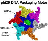
Scientists have cracked a 35-year-old mystery about the workings of the natural motors that are models for development of a futuristic genre of synthetic nanomotors that pump therapeutic DNA, RNA or drugs into individual diseased cells.
- Read more
- 421 reads
Thin films of nickel and iron oxides yield efficient solar water-splitting catalyst: Basic University of Oregon research shows promise in efforts to get hydrogen fuel from sunlight and water
- Read more
- 514 reads

NIST Mechanical Micro-Drum Used as Quantum Memory
Colorized image of NIST micro-drum and circuit on a sapphire backing. JILA researchers demonstrated that the drum might be used as a memory device in future quantum computers.
- Read more
- 440 reads
Smallest Vibration Sensor in the Quantum World
The spin of a molecule (orange) changes and deforms the nanotube (black) mounted between two electrodes (gold).
- Read more
- 422 reads
'Hot Spots' Ride a Merry-Go-Round on Jupiter

The dark hot spot in this false-color image from NASA's Cassini spacecraft is a window deep into Jupiter's atmosphere. All around it are layers of higher clouds, with colors indicating which layer of the atmosphere the clouds are in.
http://www.jpl.nasa.gov/news/news.php?release=2013-095&rn=news.xml&rst=3726
內湖2021
陳鵬程
- Read more
- 435 reads
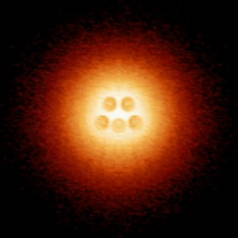
Pluto May Have 10 Undiscovered Moons

This image, taken by NASA’s Hubble Space Telescope, shows five moons orbiting the distant, icy dwarf planet Pluto. The green circle marks the newly discovered moon, designated P5, as photographed by Hubble’s Wide Field Camera 3 on July 7, 2012.
- Read more
- 436 reads
Surprising Control over Photoelectrons from a Topological Insulator: Berkeley Lab scientists discover how a photon beam can flip the spin polarization of electrons emitted from an exciting new material
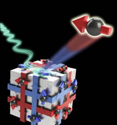
The interior bulk of a topological insulator is indeed an insulator, but electrons (spheres) move swiftly on the surface as if through a metal. They are spin-polarized, however, with their momenta (directional ribbons) and spins (arrows) locked together. Berkeley Lab researchers have discovered that the spin polarization of photoelectrons (arrowed sphere at upper right) emitted when the material is struck with high-energy photons (blue-green waves from left) is completely determined by the polarization of this incident light.
- Read more
- 450 reads
Long Predicted Atomic Collapse State Observed in Graphene: Berkeley Lab researchers recreate elusive phenomenon with artificial nuclei
An artificial atomic nucleus made up of five charged calcium dimers is centered in an atomic-collapse electron cloud.
- Read more
- 379 reads
Human Rights
Fostering a More Humane World: The 28th Eurasian Economic Summi

Conscience, Hope, and Action: Keys to Global Peace and Sustainability


Ringing FOWPAL’s Peace Bell for the World:Nobel Peace Prize Laureates’ Visions and Actions

Protecting the World’s Cultural Diversity for a Sustainable Future


Puppet Show I International Friendship Day 2020